The ABF Substrate Bottleneck
A Japanese food company controls ~95% of the insulating material inside every AI accelerator shipped today.

The package substrate rarely gets the attention of GPUs or HBM memory, but it has become one of the most important components in modern AI systems. Sitting beneath the chips, the substrate delivers power, routes thousands of high-speed connections, and holds the entire package together. As AI accelerators grow larger and more power-hungry, the substrate is increasingly becoming the motherboard inside the package—and one of the key enablers of next-generation compute.
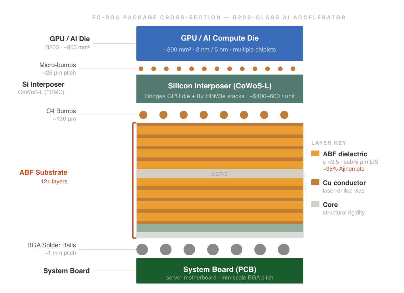
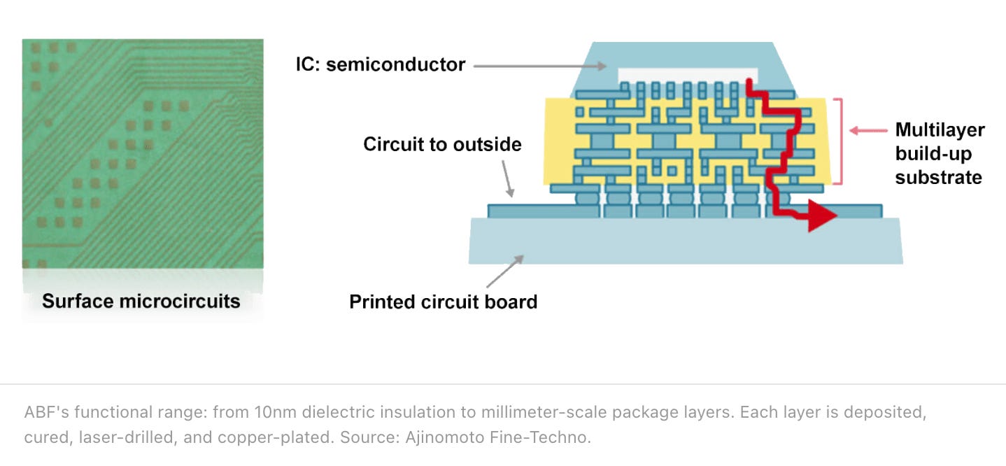
A semiconductor die cannot connect directly to a circuit board: voltage levels are incompatible, I/O pitch differs by three orders of magnitude, and thermal density would destroy the board. The substrate bridges that gap. It is constructed from alternating layers of copper conductors and ABF dielectric film — and without it, Nvidia cannot ship an H100, AMD cannot ship an MI300X, and Google cannot finish a TPU.
How a food company became AI’s silent gatekeeper
Ajinomoto Co.’s primary revenue is still food seasonings. But in 1996, Intel commissioned its chemical division to develop a film-type insulator for semiconductor packaging. Ajinomoto’s team — leveraging amino acid chemistry — delivered a working formulation in four months. Mass production started in 1999.
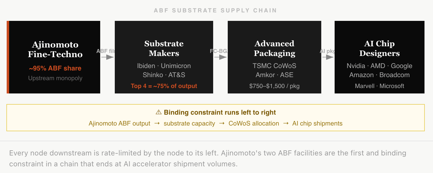
ABF has since become structurally irreplaceable. No credible alternative exists at production scale. Mitsubishi Gas Chemical and Sekisui Chemical have design wins in lower-performance applications, but neither has qualified at the layer counts or yields required for AI accelerators. Ajinomoto’s Fine-Techno subsidiary controls approximately 95% of the CPU/GPU-grade ABF market — a number that has not moved in a decade.
The moat is functional lock-in, not patents. Qualifying a new ABF supplier at a top-tier substrate manufacturer takes 18–24 months minimum. Even if a competitor produced an equivalent film today, no substrate maker could switch without halting production for Nvidia, AMD, or Intel.
Why substrates matter more than ever
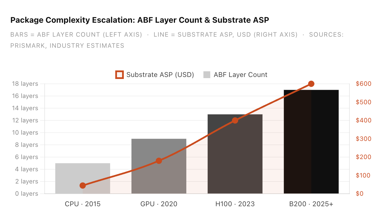
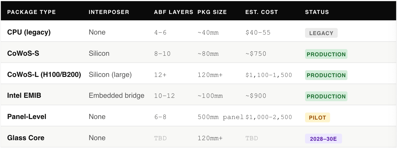
The substrate was a low-drama component. A CPU in 2015 needed 4–6 ABF layers, fit in a ~40mm package, cost $40–55, and delivered in 6–8 weeks. Three structural shifts changed this simultaneously — and none reverses.
Transistor scaling economics degraded. Moving 5nm→3nm costs 2–3× more per transistor than the prior node. The industry’s answer is chiplets: packing multiple dies from different process nodes into a single package. Every chiplet design requires a substrate, and it always needs more ABF layers than the monolithic die it replaced.
Package size and complexity exploded. An H100 GPU requires 12+ ABF layers in a package exceeding 120×120mm. Blackwell’s B200 uses CoWoS-L with a die footprint above 800mm² — among the largest packages in production history. ABF content per AI accelerator is roughly 3–4× what a CPU required five years ago.
HBM adds routing complexity. A B200 carries eight HBM3e stacks adjacent to the compute die. The substrate must fan out connections for all of them simultaneously. Each additional HBM stack adds layers, footprint, and ABF content. Hyperscale operators installed more than 1.2 million AI accelerator units in 2025.
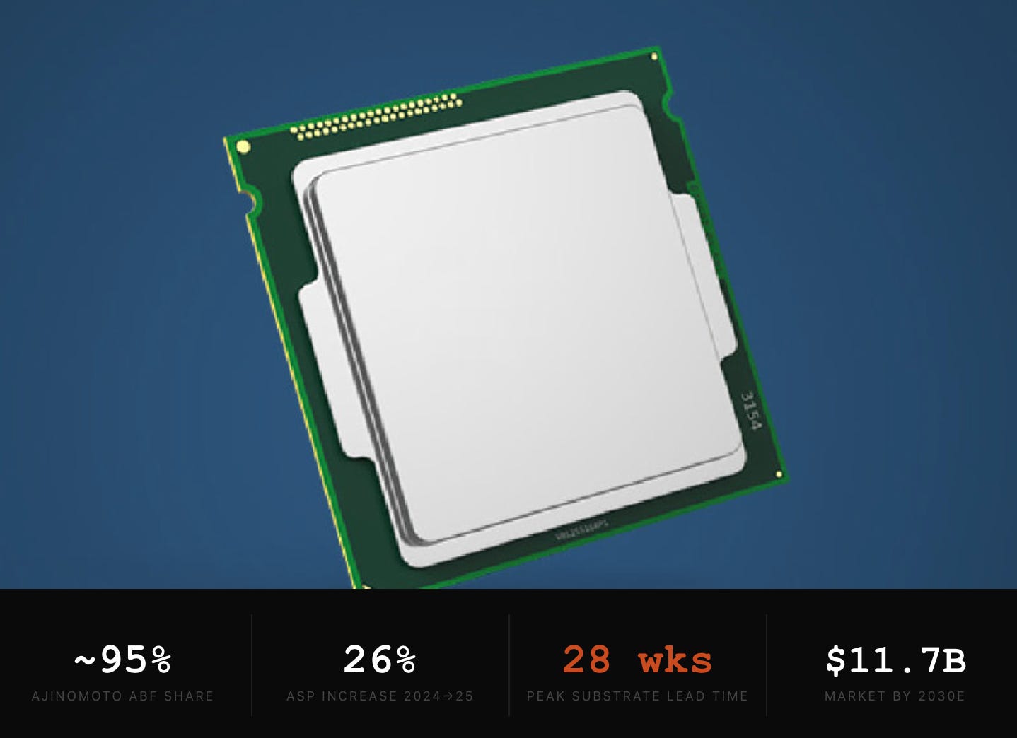
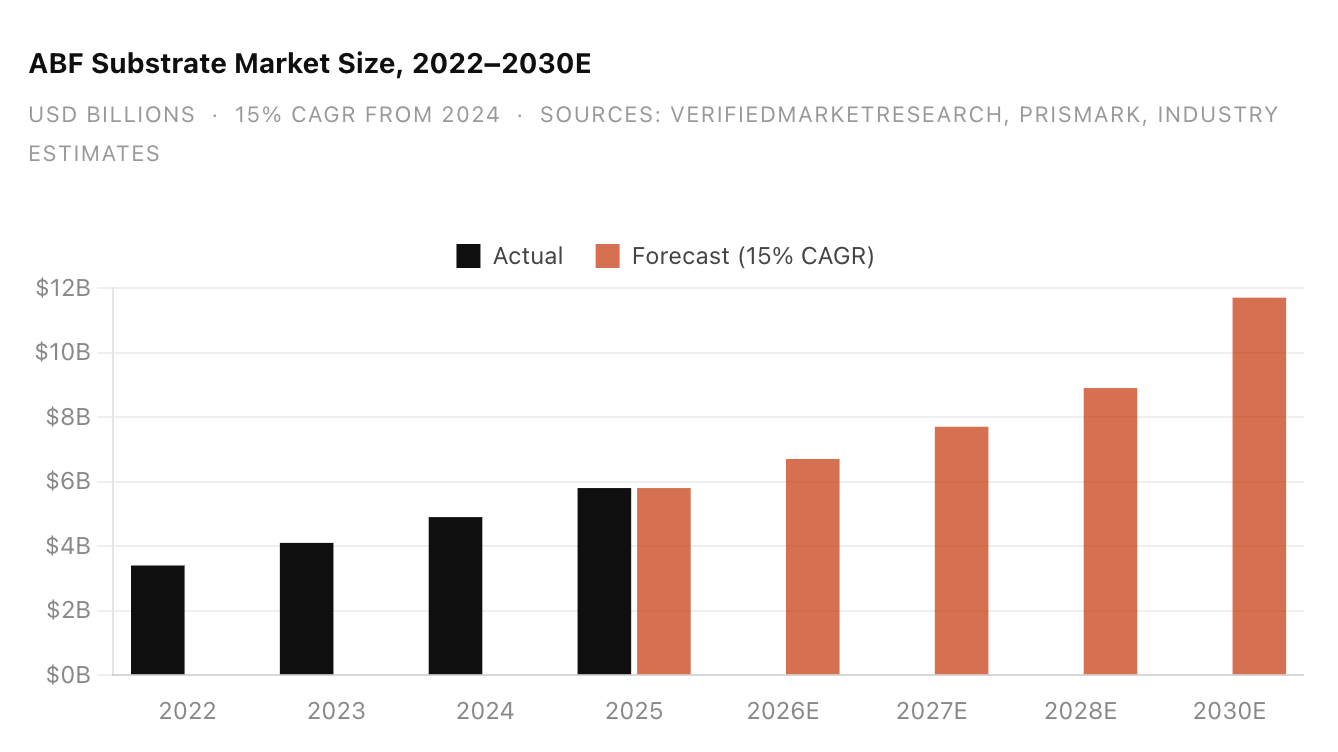
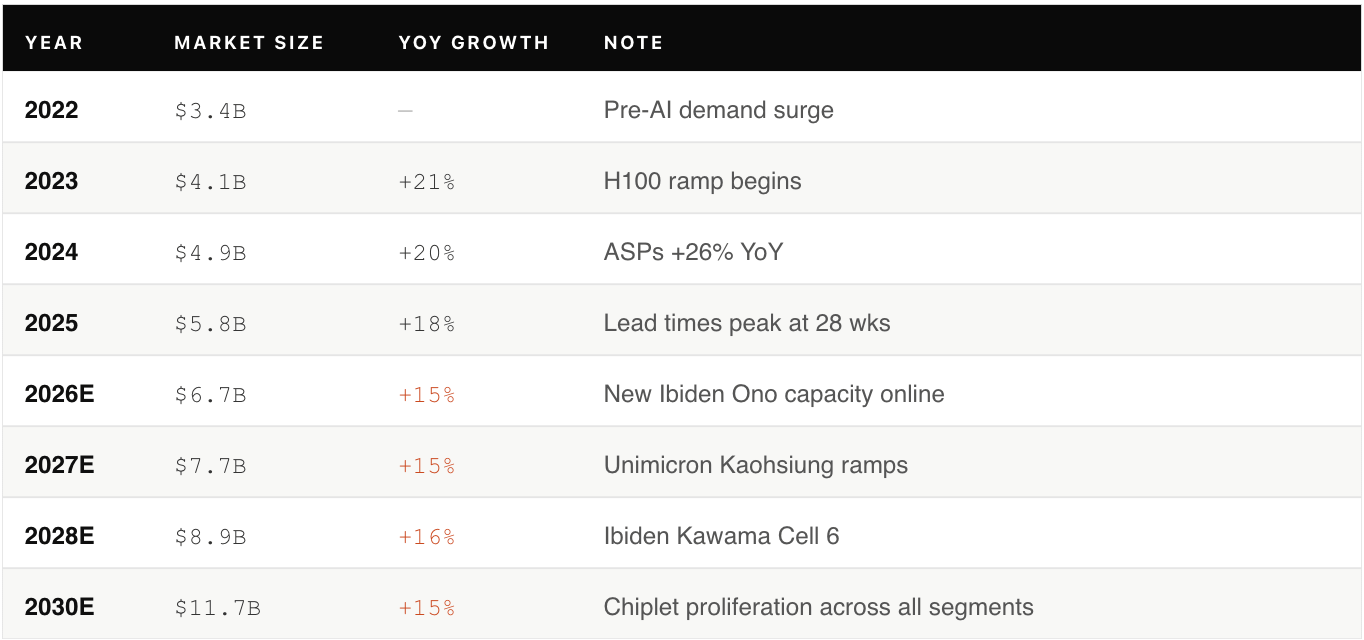
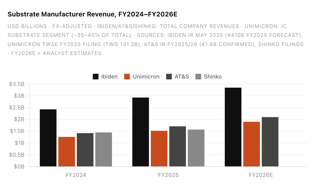
$5.8B today, $11.7B by 2030
Pricing tells the story as clearly as volume. ABF substrate ASPs rose from ~$65 (2024) to ~$82 (2025) — a 26% increase in twelve months. Lead times for 14-layer substrates peaked at 28 weeks in early 2025. Mid-tier fabless designers either paid spot premiums of 15–20% above contract or delayed tape-outs by one to three quarters.
Five companies, 82% of the market
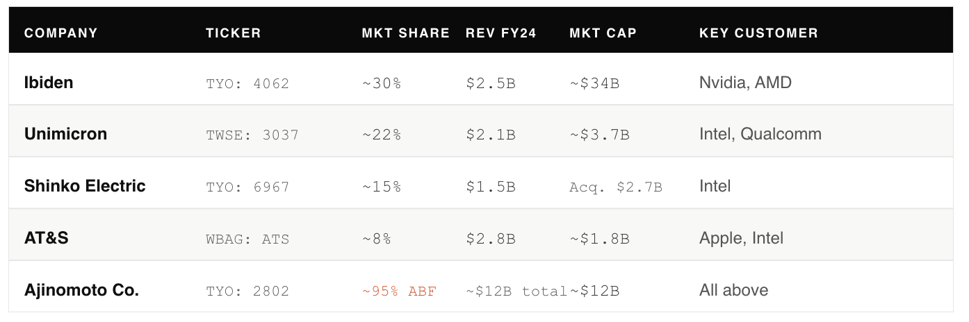
The high-end FC-BGA substrate market is split among five manufacturers: Ibiden (~35% share), Shinko Electric (~18%), Unimicron (~14%), AT&S (~10%), and Nan Ya PCB (~5%), with the remainder fragmented across smaller Asian suppliers. All five are capacity-constrained and all five have announced expansions — which obscures the more relevant fact: lead times of 20–28 weeks indicate demand is outrunning committed buildout, not just announced intentions. Shinko, majority-owned by Fujitsu, has historically been CPU-concentrated; it is now qualifying for AI workloads, but layer count limitations keep it behind Ibiden for the most complex packages.
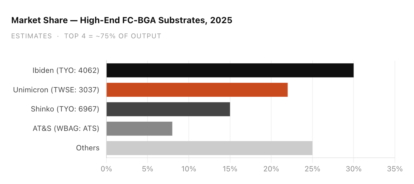
AT&S is the only European supplier at meaningful scale and has positioned itself as a geopolitical hedge, receiving EU subsidy support for its Austrian facility — strategic for customers who want non-Asian supply, but it runs at roughly one-fifth of Ibiden’s AI substrate revenue. Unimicron and Nan Ya are price-competitive at lower layer counts but have not demonstrated volume yield at 14+ layers for GPU-class packages. Ibiden’s lead is not just share — it is yield maturity at the layer counts that matter.
The substrate fab
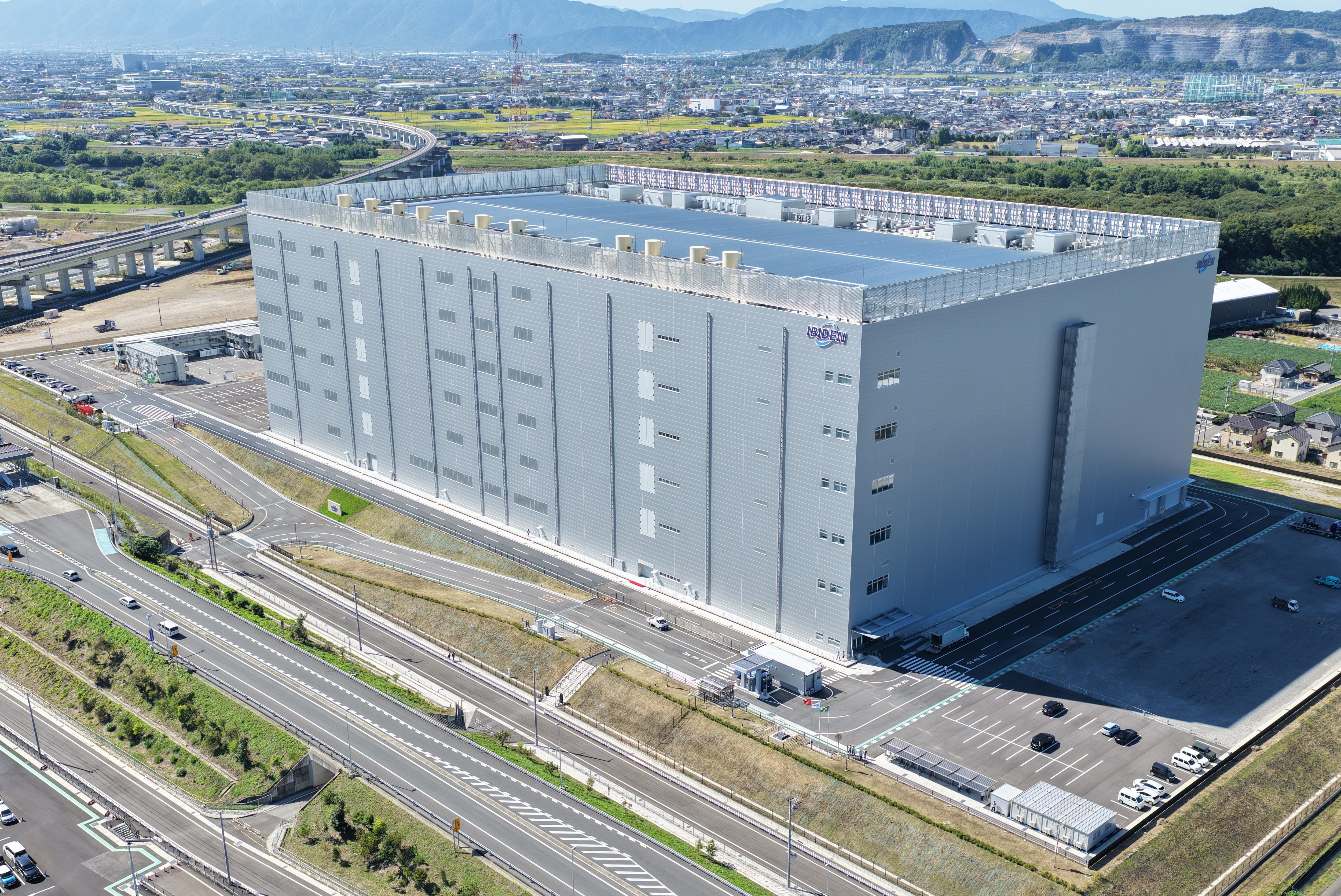
Ibiden’s ¥500B (~$3.2B) capex commitment across FY2026–2028 is the largest single substrate expansion in history. The Ono Plant opened at ~50% building utilization in October 2025. Kawama Plant Cell 6 (¥220B) targets FY2027. Combined goal: 2.5× current capacity by 2028. Demand projections from hyperscalers suggest this may not fully close the gap.
The concentration risk is unhedged: all of Ibiden’s major plants sit in Gifu Prefecture, a seismically active zone. A single facility disruption would propagate directly to AI chip shipment volumes globally. That risk has no public market hedge.
Three paths challenging the organic substrate
The interposer, panel-level packaging, and glass core substrates converge on the same problem — but on different timelines, with different ABF implications.
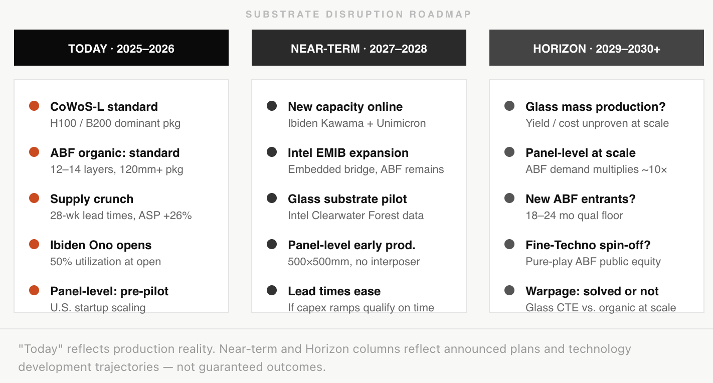
Glass substrates and the Corning bet
The problem glass solves is warpage. Organic ABF substrates deform above ~120×120mm packages because of CTE mismatch between the film (~30 ppm/°C) and the silicon die (~2.6 ppm/°C). During reflow, the package warps — the “potato chip” effect — causing yield loss that compounds as die size grows. Every generation of AI GPU package pushes toward or past this limit.
Glass CTE can be engineered between 3–9 ppm/°C, far closer to silicon. It enables finer via density, lower signal insertion loss, and better flatness for lithographic patterning. If glass qualifies at volume, it directly displaces ABF as the substrate dielectric — a long-dated but high-conviction risk for Ajinomoto Fine-Techno.
The timeline risk is real. Glass substrates require entirely new manufacturing equipment, process qualification at multiple yield gates, and supply chain infrastructure. Mass production below $500/substrate is not demonstrated at scale. ABF organic remains the production standard through at least 2028, and likely longer for the majority of the market. Corning is the clearest public equity read-through — but the transition is multi-year, capital-intensive, and yield-dependent.

The ABF control point the market underprices
The substrate layer is one of the few places in AI infrastructure where non-semiconductor companies exercise structural leverage over hyperscaler capex. Ibiden can constrain Nvidia’s shipment volumes. Ajinomoto constrains Ibiden.
The market treats substrate manufacturers as contract manufacturers — process-intensive, capital-heavy, margin-thin. That framing made sense when substrates were commodity components. It does not describe a company whose yield curve at 14+ ABF layers determines whether Blackwell ships on schedule.
Ajinomoto Fine-Techno illustrates how durable that leverage is. A food company’s chemical division holds 95% of the most upstream material input in AI compute — not through patents or price, but through an 18–24 month qualification barrier that no substrate maker can absorb without halting production for its largest customers. That is a control point maintained entirely by switching cost.
The pattern repeats across the production chain. The companies that dominate AI market cap are not always the companies that hold structural leverage. The further you trace the physical stack, the more single-point dependencies you find — held by companies that most AI coverage never mentions.