

What does TSMC do?
Discussing the paramount player in the semiconductor supply chain: covering business model, founding story, customers and competitors, the role of AI, and its US expansion

The semiconductor industry has the deepest and most complex supply chain in the global economy. TSMC sits at the crux of this as the 10th most valuable company in the world, with the $500B+ giant serving every technology company in the top 10 most valuable companies globally (Apple, Microsoft, Google, Amazon, Nvidia, Meta and Tesla). TSMC is undoubtedly the most strategic company in Asia, making up over 15% of Taiwan’s GDP, producing over 60% of the world’s semiconductors and over 90% of advanced semiconductors. In many ways, TSMC is an index on the semiconductor industry — from mobile to the data center and new technologies like auto. As such, TSMC provides key insights on the future of these sectors.

Semiconductors and advanced chipmaking are the “Space Race” of modern times. As the industry most affected by trade agreements between the US and China, the world became aware of diversifying supply chains and the risks in semiconductors with COVID-19. As the sole maker of advanced AI chips, TSMC and the semiconductor industry are called Taiwan’s “silicon shield” — uniting the world around a reason to defend the Island from blockade or invasion. TSMC, aware of these geopolitical risks, has moved to diversify manufacturing outside the island, announcing hundreds of billions of dollars of new plants outside Taiwan.

Tim Cook joins TSMC founder Morris Chang and management, along with Joe Biden to announce $40B US Chip Venture
What makes TSMC the dominant player that it is with >90% market share in advanced chips? In short, a unique business model coupled with operational excellence and high investment in cutting edge technologies. As AWS and Azure allowed software companies to outsource server infrastructure to instead focus on designing software, TSMC allowed semiconductor companies to outsource manufacturing to instead focus on chip design. Both birthed thousands of new companies by reducing capital investment and barriers to entry.
We dive in below.
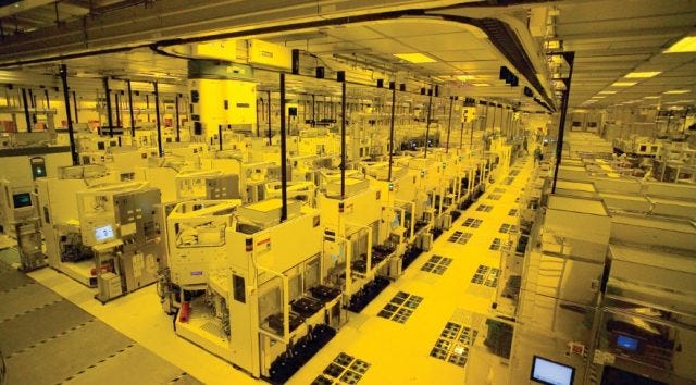
What are semiconductor “fabs”?
Semiconductor "fabs," short for fabrication facilities, are the heart of the semiconductor manufacturing process, where integrated circuits, or chips, are created. These fabs are essentially advanced manufacturing facilities equipped with cutting-edge machinery (from companies like ASML for EUV, Applied Materials and Lam Research for etching and materials, KLA for process control, etc. — see more here) and clean rooms to produce semiconductor wafers. What sets TSMC (Taiwan Semiconductor Manufacturing Company) apart from other key players like Intel and Samsung in the semiconductor manufacturing industry is its unique business model as the first pureplay fab and integrated circuit foundry in the world.

Source: TSMC to triple U.S. chip investment to $40B, with the Arizona plant depicted
TSMC is often referred to as a "pure-play" foundry, which means its primary focus is on contract manufacturing of semiconductors — introducing this concept in 1987 at its founding. Unlike Intel and Samsung, who also design and manufacture their own chips, TSMC exclusively specializes in manufacturing chips designed by other companies. This specialization allows TSMC to dedicate its full resources to semiconductor manufacturing production and processes — resulting in better cost/performance and quality output. TSMC's fabs are renowned for their world-class precision, cutting-edge process nodes, and commitment to innovation, making them the go-to choice for many semiconductor designers looking to bring their chip designs to life. This unique business model and relentless pursuit of semiconductor manufacturing excellence position TSMC as the key leader in its industry.
In time, though, TSMC got better, in large part because it had no choice: soon its manufacturing capabilities were only one step behind industry standards, and within a decade had caught-up (although Intel remained ahead of everyone). Meanwhile, the fact that TSMC existed created the conditions for an explosion in “fabless” chip companies that focused on nothing but design…the increased business let TSMC invest even more in its manufacturing capabilities.
— Ben Thompson, Chips and Geopolitics
The complexity of these fabs can’t be overstated — with even the $500B+ market leading giant only operating 18 total fabs. All but 3 of these fabs are operated in Taiwan, with one additional fab in WA state and two fabs in China — though more fabs are being built now in the US with TSMC tripling its US investment. Each fab often involves investments of at least $5B and up to $60B, between clean room facilities, highly specialized equipment and infrastructure. The higher cost fabs tend to focus on more advanced technology nodes like 3nm and 5nm which squeeze more transistors on each chip and drive higher compute performance. Each plant typically has ~10K R&D personnel, bringing high quality jobs to the regions plants are built.
Source: TSMC
Founding History and Differentiation
Perhaps surprisingly, TSMC was only founded just over 30 years ago by Morris Chang. Having founded the company at age 57, Chang had a storied career in the semiconductor industry in the US before ultimately deciding to return to Asia. He grew up in China and Hong Kong, but came to the US to attend MIT and later went on to get a PhD from Stanford. His storied career in the semiconductor industry consisted of 25 years at Texas Instruments as he rose up to become a VP at the now $150B US company. Notably, he pioneered the then controversial idea of pricing semiconductors “ahead of the cost curve”, which meant sacrificing early profits (“short term”) to gain market share and achieve manufacturing yields that would result in greater profits over an extended time (“long term”). In the 1970s, when TI’s focus turned to calculators, digital watches and home computers, he felt like his career was at a dead end at TI.

While at Texas Instruments, Chang witnessed TI’s factory in Japan achieving twice the chip production yield as TI’s factory in Texas. He observed that the staff and technicians in Japan are better qualified and had lower turnover, with recruiting quality technical staff far easier than the US. Chang determined the future of semiconductor manufacturing was in Asia and started TSMC in 1987, three decades after he left during the chaotic Chinese Civil War.

Intel had invented the microprocessor in 1971 and dominated the general purpose computing market over the next few decades. By integrating software, design, and manufacture from the 1970s — Intel dominated the market. Intel designed its processors to be general; however, processors that were made for specific tasks could be much faster, at least in theory. Chang picked up on this opportunity at Texas Instruments in the 1980s, but identified the key challenge in getting started — the barriers to entry in founding a chip company costing $50-100M+ to start, mainly because of manufacturing costs. At the time, new chip companies could contract with Texas Instruments, Intel or Motorola — though reliability wasn’t strong and they were your direct competitor. This was the key business model innovation in the pureplay foundry — no upfront fixed cost, no competition from your supplier. Chang made it possible for chip designers to start their own companies built around IP in chip design.
When I was at TI and General Instrument, I saw a lot of IC [Integrated Circuit] designers wanting to leave and set up their own business, but the only thing, or the biggest thing that stopped them from leaving those companies was that they couldn’t raise enough money to form their own company. Because at that time, it was thought that every company needed manufacturing, needed wafer manufacturing, and that was the most capital intensive part of a semiconductor company, of an IC company. And I saw all those people wanting to leave, but being stopped by the lack of ability to raise a lot of money to build a wafer fab. So I thought that maybe TSMC, a pure-play foundry, could remedy that. And as a result of us being able to remedy that then those designers would successfully form their own companies, and they will become our customers, and they will constitute a stable and growing market for us.
— Morris Chang, TSMC
Graphics processors were an early example of a new vintage of “fabless” companies: Nvidia was started in 1993 with only $20 million and never owned a fab. Qualcomm and IBM spun off manufacturing units to concentrate on design, while Apple started building its own chips without a fab a decade later. Silicon Graphics and AMD were other players that emerged with new architectures. Today there are thousands of chip designers in various industries from aerospace, to automobile, mobile and the data center — with none operating their own fabs.
TSMC’s Business Today
One thing to appreciate about TSMC is its investor materials, which are all substance and zero design. The Company forecasted $18.5B of revenue for the first quarter of 2024, bringing annualized revenue to nearly $75B and ~25% forecasted growth. Despite being a capital intensive company, TSMC operates at 57% gross margins — and nearly everything after that is profit with 45%+ operating margins. The Company has averaged ~16% annual revenue growth for the past 5 years and has lifted its EBIT margin by ~10% over the same period.

The Company has guided towards mid 20s % growth in 2024 and ~19% growth in 2025. This exceeds even cloud vendors like Amazon, Microsoft and Google, as well as the semiconductor space as a whole

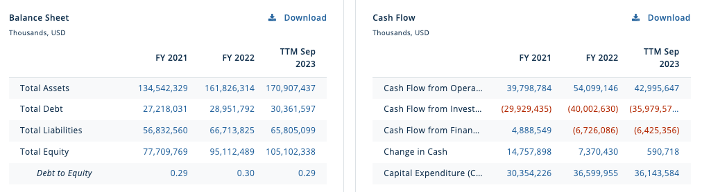
As an operator of some of the most complex semiconductor facilities in the world with high technology equipment, TSMC has a complex balance sheet and cash flow statement — though has very little debt. It’s continually reinvesting cash flow from operations into new facilities, though is stacking more cash each year.
TSMC’s two main segments are smartphones (where Apple is its largest customer and accounted for 23% of total TSMC revenue by many estimates) and high performance computing (HPC where customers include Nvidia, AMD and Broadcom in the data center) — which each account for ~43% of revenue.

TSMC claims its top 10 customers collectively hover around ~70% of total revenue. The Company’s 10 largest customers (in rough order of magnitude) are Apple, Nvidia, AMD, Qualcomm, Broadcom, Mediatek, Intel, NXP, Amazon and Microsoft.
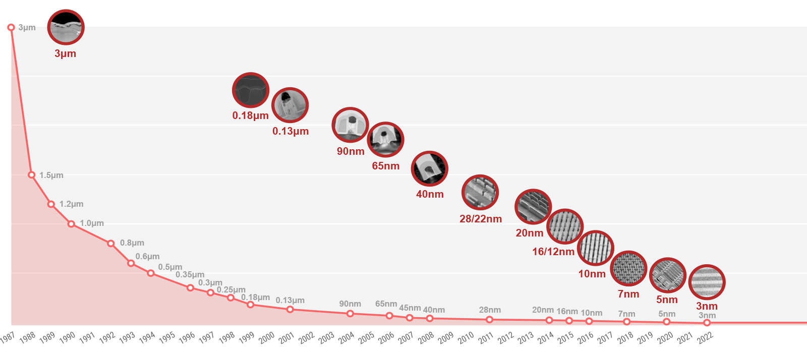
As mentioned above, TSMC defines its revenue by technology and end segment. Each fab services different nm chips — with 3nm and 5nm contributing most of the growth for TSMC. TSMC generates over 50% of its revenue from these type of nodes, which are highly advanced and it faces fewer competition and over 67% from advanced nodes (7nm and below).

TSMC makes ~70% of its revenue from North America, with the rest being split across China (~10%), APAC (~8%), Europe (~6%) and Japan (~5%).

Competitors and Differentiation
As Dan Nystedt points out, the shift towards 3nm technology has dramatically increased TSMC’s 12-inch wafer prices, which have more than doubled since 2018. Competitors are far behind TSMC on 3nm and advanced chips, which drive most of industry growth that explains TSMC’s gaining market share of the overall manufacturing market. TSMC is >60% of the overall semiconductor manufacturing market share and >90% for advanced computing.

Its closest competitors are Samsung Electronics (who has been losing market share recently), GlobalFoundries and UMC.

Source: Eric Flanigan [link]
TSMC differentiates from competitors with its operational excellence and constant push towards new nodes that lower nm. This thread on YC discusses some areas of differentiation. Though all players use similar equipment from ASML, Applied Materials, Lam Research, KLA and others — the processes, staff, facilities and capital investment strategies are quite different in practice. TSMC is simply run better.
CoWos as the bottleneck for AI Chipmaking
It’s no secret AI is capacity constrained. As Semi Analysis shares in this piece, the biggest bottleneck in the supply chain is CoWoS capacity (“Chip on Wafer on Substrate”). CoWoS is an advanced semiconductor packaging technology that enables multiple chips to be stacked vertically on a single substrate, improving performance and power efficiency in integrated circuits.
The vast majority of CoWoS demand comes from AI, with Nvidia alone accounting for over 50% of all orders. CoWoS is a key innovation for AI because it enables the integration of multiple high-performance chips onto a single substrate, optimizing power efficiency and bandwidth, which is particularly crucial for AI applications. Nvidia and AMD use CoWoS to enhance the performance of their GPUs and accelerators by tightly stacking memory and logic chips, reducing data transfer bottlenecks and accelerating AI computations.
TSMC has plans to double its CoWoS output this year and will grow capacity >50% YoY until at least 2027 per management guidance [link]. Even as TSMC accelerates CoWoS capacity and raising expansion for customers like Nvidia and AMD, it can’t keep up with customer demand. H100 lead times are still 10 months.
Semi Analysis built a bottoms-up model to estimate CoWoS demand across TSMC customers, which serves as a proxy for AI chip demand. See below for this.

The Future: US Expansion Plans and the CHIPS Act
With the passage of the CHIPS Act in August 2022, the US authorized roughly $280 billion (!) in funding to boost domestic R&D of semiconductors across a variety of initiatives:
$39B in semiconductor manufacturing
25% investment tax credits in manufacturing equipment
$13B for research and workforce training
$174B in public sector research including NASA, DOE, NIST
The importance of this macro backdrop within the chip sector can’t be understated. It is perhaps equally as important as the shift to AI and more demanding chips. Since the announcement of the CHIPS act, the SOXX Semiconductor Index has appreciated by over 60%, more than 4X that of the S&P500.
After opening its first facility in Washington, TSMC announced a $40B facility in Arizona which will bring tens of thousands of semiconductor jobs to the region. This plant will be operational in 2027 or 2028. TSMC will also open its first fab in Japan next month. Last year, it announced its first factory in Europe in Dresden, Germany.
