

The Memory Triopoly
How SK Hynix, Samsung, and Micron became AI's most concentrated control point — and why HBM is >50% COGs of every Nvidia GPU sold.

We’ve been talking a lot about memory lately — from KV Cache dynamics across prefill and decode to memory itself as the structural bottleneck in AI compute. The constraint is no longer raw FLOPS. It is the ability to move bytes in and out of those FLOPS fast enough to keep increasingly massive models fed.
Three companies — SK Hynix, Samsung, and Micron — own that bottleneck. They control approximately 96% of DRAM and effectively 100% of High Bandwidth Memory (HBM). HBM is now the single most economically critical component inside Nvidia’s accelerators, contributing >50% of the bill of materials of a Blackwell Ultra (B300) and rising further on Rubin. Historically a cyclical industry, memory suppliers are seeing above prior peak-cycle gross margins today in excess of 70%.
At peak-cycle HBM economics, SK Hynix is beginning to outearn the hyperscaler businesses like Meta that buy their products. Combined, the memory triopoly is projected to generate 2–3x Meta’s net income in 2026.
Compute Scales Faster Than Memory
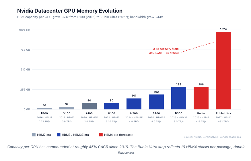
Every Nvidia generation has run into the same wall: memory. Memory capacity per GPU grew ~18x from P100 to Rubin Ultra in 11 years. FP compute grew approximately 500x over the same period.
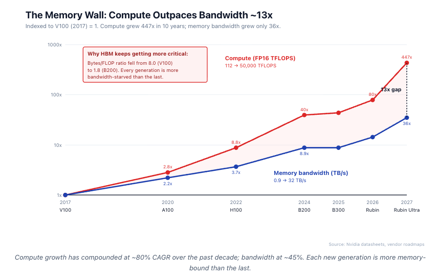
The implication is structural: every successive AI generation becomes more bandwidth-constrained. Memory has gone from ~20% of GPU BOM (A100) to ~55% (B200). For Rubin, HBM may exceed the cost of the logic die itself. We are beginning to approach physics limits with how much HBM can be placed on the processor. GPU shoreline is fixed by die perimeter, and HBM stacks can only sit along two of the four edges — which is why Rubin Ultra moves to 16 stacks by going taller, not wider.
HBM Bill of Materials and Margin Capture
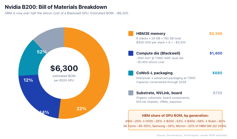
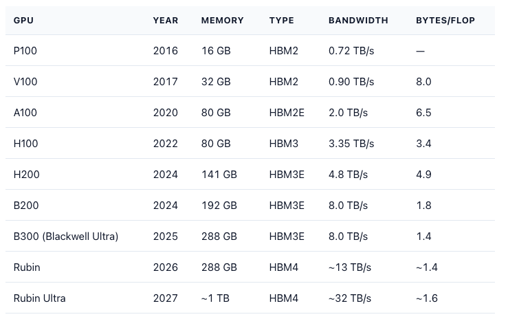
A B200 has 8 HBM3E stacks at 24 GB each (192 GB total). HBM share of GPU BOM is ~52% on B200, ~58% on B300 (Blackwell Ultra, 288 GB HBM3E 12-Hi), and tracking ~62% on Rubin (HBM4) based on early ASP guides.
Nvidia sells B200 at $30,000–40,000 list. Of every incremental B200 dollar, roughly $0.10–0.15 flows to HBM suppliers as gross margin contribution. SK Hynix captures ~45–50% of that. Samsung ~30%. Micron ~22%.
Memory suppliers are now tied to Nvidia’s revenue trajectory more tightly than perhaps any supplier-customer relationship in modern semiconductor history.
Cost per Gigabyte: The Brutal Hierarchy
Memory is not one market. It is a stratified stack with six orders of magnitude in cost difference.
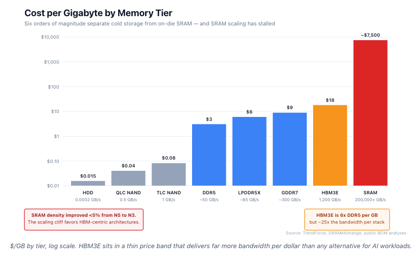
HBM3E is ~6x DDR5 per gigabyte but ~25x the bandwidth per stack. On a $/(GB·bandwidth) basis, HBM is the only economically rational choice for AI workloads above a certain compute density.
SRAM is two to three orders of magnitude more expensive than HBM per gigabyte. And SRAM scaling has stalled. From TSMC N7 to N5, SRAM density improved 5%. From N5 to N3, less than 5% again. The historical assumption that on-die cache would keep up with logic has failed.
This is the SRAM scaling cliff. Every AI architecture that depends on large on-die caches (Cerebras, Groq-style approaches) faces an increasingly hostile cost curve. HBM remains the only memory technology that combines large capacity, high bandwidth, and acceptable cost.
The Memory Wall, Quantified
AI’s core architectural problem is no longer compute scarcity. It is memory starvation.
AI workloads are bound by three physical constraints, not by FLOPS:
Modern GPUs require far more compute per byte than transformer workloads naturally generate. Every GPU has a balance point — how many math operations it can do for each byte of memory it can fetch. For V100 (2017) the balance point was ~125 FLOPS per byte. For B200 today it is ~560 FLOPS per byte. To run the GPU flat-out, software needs to do that many operations on each byte it touches. Transformer decode workloads fall dramatically short of that threshold. Typical decode workloads only do 1–10 operations per byte fetched — they spend most of their time waiting on memory. The result: AI silicon often runs at 15–35% of peak FLOPS during inference. Every additional TB/s of HBM bandwidth converts directly into utilization recovery and lower cost-per-token.
KV cache now dominates inference memory. During inference, every prior token’s “key” and “value” representations have to stay in memory for the next token to attend to them. This is the KV cache, and it grows with context length × batch size. Llama 3 70B at 128K context with batch size 32 needs ~80 GB just for KV cache — more than the model weights themselves. At 1M context, KV cache exceeds 600 GB per request. This is why H200’s 141 GB and B200’s 192 GB are a step change versus H100’s 80 GB: not because the weights got bigger, but because the cache did.
Moving data costs more energy than doing math on it. Moving one bit across HBM costs about 7 picojoules. Across off-package DDR5: 80 pJ. From on-die SRAM: 0.1 pJ. Doing an 8-bit multiply on a 4 nm node: 0.05 pJ. At trillion-operation inference scales, data-movement energy exceeds compute energy by 3–10x.
This is why every architectural response — HBM4 with logic base dies, stacked SRAM, processing-in-memory — is fundamentally about reducing joules-per-byte moved.
The economic translation: HBM bandwidth is the highest-leverage capex decision in AI infrastructure. For modern transformer workloads, the marginal value of additional HBM bandwidth often exceeds its marginal cost.
What an HBM Stack Actually Is
? Deep Dive into Architecture, Packaging, and Applications")
Source: High-Bandwidth Memory, Semi Engineering
Before getting into vendor differences, a quick engineering picture. HBM isn’t a chip — it’s a small skyscraper of chips.
An HBM3E 12-Hi stack is twelve DRAM dies sitting on top of a logic base die. Each DRAM die is ground down to about 30 μm thick — roughly a third of a human hair — so the whole tower fits inside the package. The dies are connected vertically by through-silicon vias (TSVs): copper-filled holes drilled through each die, 5–10 μm wide and spaced ~50 μm apart. A 12-Hi stack has 1,200–1,800 TSVs per layer for data and power, plus thousands more for signal integrity.
The stack sits next to the GPU compute die on a silicon interposer. The interposer is the wiring layer that carries the 1,024-bit (HBM3) or 2,048-bit (HBM4) bus between memory and compute at trace densities and impedances that organic substrates can’t match. For Nvidia accelerators, the relevant implementation is TSMC’s CoWoS-L.
Three things make HBM hard to build:
Heat. Each stack dissipates 4–8 watts. That heat has to escape upward through twelve thin silicon layers and the adhesive between them. The thermal limit is why H100 launched in 2022 with only five of six possible HBM3 stacks active — the sixth bay was reserved as thermal and yield margin.
Yield compounds. A single bad TSV kills the entire stack. At 99% per-die yield, a 12-Hi stack yields 88.6%. At 95% per-die, only 54%. This is why per-die yield matters more than headline density at HBM scale — and why SK Hynix’s 75–80% 1bnm yield is a wider competitive moat than the number alone suggests.
Wider IO beats faster IO. HBM4 doubles the interface from 1,024 to 2,048 bits but keeps the per-pin speed roughly the same as HBM3 (~6.4 Gbps). Wider-and-slower uses less power per bit and yields better than narrower-and-faster at modern interposer densities. This single choice forces the base die onto a logic foundry node (TSMC N5/N3) instead of a DRAM line and determines which vendors can build it.
There are two ways to physically stack the dies:
MR-MUF (Mass Reflow with Molded Underfill) — SK Hynix’s proprietary method. Bond and fill the gaps between dies in a single thermal cycle. Better heat conduction, fewer voids between layers.
NCF (Non-Conductive Film) — Samsung’s method. A pre-applied film is bonded layer-by-layer. Cheaper equipment, slower per stack, lower yield historically. Samsung’s revised “Advanced TC-NCF” closed but did not eliminate the gap for HBM4.
Layer count keeps climbing. HBM4 supports 16-Hi configurations — double what HBM3 launched at. The earlier 720 μm packaging ceiling could not accommodate 16-Hi stacks, forcing the standard to expand to 775 μm in late 2024. The taller envelope means microbumps remain viable for HBM4, and the long-anticipated transition to direct copper-to-copper bonding has slipped to HBM4E or later.
Once copper-to-copper bonding arrives, interconnect pitch shrinks dramatically while removing the bump gap between dies entirely — enabling higher stack density and lower power per bit. The tradeoff is a new bottleneck: hybrid bonding tool capacity.
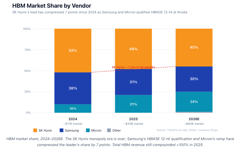
HBM market share, 2024–2026E. The SK Hynix monopoly era is over; Samsung's HBM3E 12-Hi qualification and Micron's ramp have compressed the leader's share by 7 points. Total HBM revenue still compounded >100% in 2025.
The Triopoly in Numbers
DRAM is a triopoly. HBM is no longer a SK Hynix monopoly — Samsung’s HBM3E 12-Hi qualification at Nvidia in Q4 2025 and Micron’s ramp have compressed the leader’s share by ~7 points in 18 months. But total HBM revenue continues to compound at >70% YoY, so all three are growing absolutely.
Through five DRAM cycles since 2010, the industry consolidated from 10+ vendors to three. Each downturn pushed marginal capacity out. The result is the highest sustained pricing power in the history of memory: HBM3E ASPs are 6–8x conventional DDR5 per gigabyte, HBM4 ASPs are ~10x, and capacity remains fully sold out through 2027.

SK Hynix — The HBM Leader
The #1 HBM supplier at ~45% share, sole supplier of HBM3 to Nvidia’s H100, and now the lead supplier of HBM4 into Rubin.
The technical moat is two-fold. SK Hynix’s 1bnm DRAM yield runs 75–80%, versus Samsung’s 60–65% on 1cnm — a gap that compounds across 12 stacked dies. Its proprietary MR-MUF stacking process keeps it alone above 80% yield on HBM3E 12-Hi.
Looking forward: SK Hynix shipped first HBM4 12-Hi samples to Nvidia in March 2026 — a 6–9 month lead over the competition into the Rubin socket. The HBM4 base die is fabricated at TSMC N5, coupling the memory and logic moats at the most advanced node.
Main risk: Nvidia is ~42% of total revenue, the tightest single-customer relationship in modern semiconductors.
Samsung — The Vertically Integrated Comeback
The largest memory company by capex, but it lost the HBM3 cycle. Thermal failures at Nvidia in 2023, yield misses at the 1anm node, and slower TC-NCF stacking left Samsung well behind.
The story flipped in 2026. 1cnm DRAM yields converged to ~65% in Q1 2026. HBM3E 12-Hi qualified at Nvidia in November 2025. “Advanced TC-NCF” closed the stacking gap. And AMD’s MI400 is now committed primarily to Samsung HBM4 — the first major AI socket Samsung has fully won this cycle.
The structural advantage no one else has: Samsung is the only memory company that also owns its own logic foundry. As HBM4E moves to customer-specific logic base dies in 2027, Samsung can co-design memory and base die without crossing a corporate boundary.
Main risk: Still 6+ months behind SK Hynix on HBM4. The HBM4E generation in 2027 is where Samsung’s integration thesis actually has to prove out.
Micron — The American Hedge
The smallest of the three, but with two distinct advantages.
A different DRAM cell architecture. Micron uses an “open bit-line” topology with vertical capacitors where SK Hynix and Samsung use planar designs. Micron claims ~30% lower active power on HBM3E at the same bandwidth (vendor-published, directionally credible).
US production. Micron is the only material DRAM manufacturer with US fabs. Idaho ID-1 opened October 2025; the New York Clay megafab was pulled forward to 2027. A $6.1B CHIPS Act grant and $7.5B in loans underwrite a multi-decade capex floor that no Asian competitor has.
Looking forward: HBM3E 12-Hi shipping into B300 since Q4 2025. HBM4 sampling at Nvidia in Q2 2026, volume H1 2027 — roughly parity with Samsung, ~6 months behind SK Hynix. HBM has gone from <2% of Micron revenue two years ago to ~26% today — a faster mix transition than either competitor went through.
Why Not More Players?
Greenfield DRAM fab cost in 2024: $15–25B. Lead time: 4–5 years. Yield ramp: 18–36 months. HBM-specific packaging capex (TSV, CoWoS-equivalent): another $2–5B per node.
Total cumulative capex required to enter the HBM market at material scale (10% share): ~$30–50B. Time required: 7–10 years.
No new entrant is plausible. Chinese efforts (CXMT, YMTC) are 3–5 nodes behind and structurally blocked from EUV. Indian, Japanese, and Taiwanese efforts are early-stage. The triopoly is durable for at least a decade.
Structural Observations
Not investment recommendations. Five things to track across the cycle:
SK Hynix’s HBM4 lead is the highest-margin product in memory history. Watch Nvidia concentration (42% of revenue) and hyperscaler dual-sourcing — visible already on AMD MI400 (Samsung) and Trainium 3 (Micron + Samsung).
Samsung’s recovery is data-supported, not speculative. 1cnm yield convergence, HBM3E 12-Hi qualification, and the MI400 win ended the “structurally behind” thesis. Open question: does foundry-plus-memory integration matter at HBM4E?
Micron has crossed from optionality to fundamentals. Fully booked HVM through 2026, 24% share, CHIPS Act margin floor. Main risk is HBM4 schedule slip.
TSMC is the silent fourth participant. CoWoS-L sold out through 2027 despite ~3x capacity expansion. Memory and logic moats are now coupled at the most advanced node.
Equipment vendors capture proportional margin. HBM capex intensity per wafer is 3–5x prior DRAM cycles — flowing to lithography, TSV etch, deposition, and hybrid-bonding tools.
Where Startups Are Trying to Break In
A wave of startups is either trying to route around HBM or build new abstractions on top of it. Three categories matter.
Memory Processing Units (MPUs). Compute placed inside the memory array itself, so data never has to cross the package. The architectural bet: as data movement comes to dominate energy and latency, the chip’s center of gravity shifts toward memory with compute as the satellite. Several early-stage startups have tested working silicon on this concept, but the category remains pre-commercial — useful as a forward indicator of where the industry may head, not yet a commercial threat to HBM.
Custom HBM-plus-SRAM accelerators. Transformer-specific ASICs that combine HBM for capacity with oversized on-die SRAM for bandwidth. Cerebras WSE-3 carries 44 GB of on-die SRAM at 21 PB/s aggregate — no HBM at all. Groq’s LPU goes further with ~230 MB SRAM per chip and statically schedules weights across hundreds of chips. MatX pairs HBM3E/HBM4 with large on-die cache, betting that workload specialization can beat Nvidia’s general-purpose silicon on tokens-per-dollar.
Memory fabrics. Connective tissue around memory rather than memory itself. Astera Labs (CXL switches and memory expanders, now public) leads the commercial wave. Eliyan’s NuLink offers organic-substrate chip-to-chip interconnect competitive with silicon interposers — potentially loosening TSMC’s CoWoS chokepoint. Enfabrica is building a converged network-and-memory fabric that pools HBM and DDR across a rack. Celestial AI is pushing photonic interconnects with claims of 10–100x lower energy per bit between memory and compute.
None of these displaces HBM as the bottleneck. Each either accepts HBM as the foundation and extracts more performance around it, or routes around HBM in workloads narrow enough for SRAM to substitute. That is exactly why the triopoly remains durable.
Summary
The memory triopoly is the most concentrated, most capital-intensive, most expensive chokepoint in the AI server. HBM is now 50%+ of accelerator BOM. Memory bandwidth grows ~2x per Nvidia generation while compute grows 5–10x. The gap widens. The triopoly captures the margin.
Nearly every architectural response — HBM4 logic base dies, stacked SRAM, PIM, MPUs, CXL fabrics — ultimately reinforces the same bottleneck. The next decade of AI capex driven by Nvidia and TSMC flows into the memory triopoly more than into any other layer of the stack.
The bottleneck is the moat.